
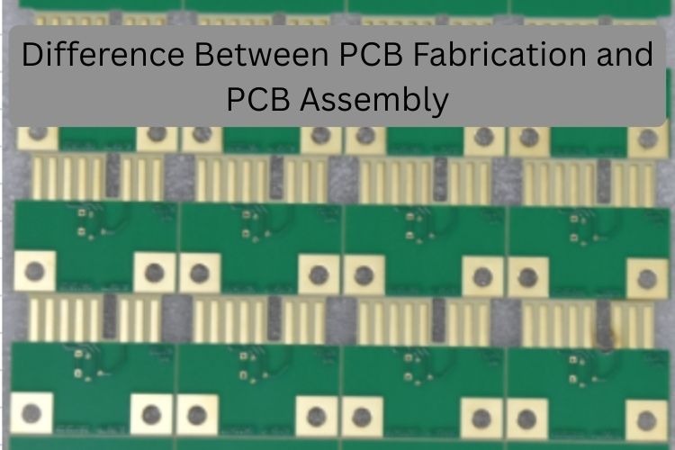
What is the Difference Between PCB Fabrication and PCB Assembly?
PCB assembly and PCB fabrication are used interchangeably, yet there is a difference between the two phases in the development of an electronic product. Having knowledge of their variations will allow you to budget, plan, and allocate vendor task in a more smart way particularly when you are outsourcing entire pcb fabrication and assembly services to manufacture run.
What Is PCB Fabrication?
The process of conversion of your design files into a fabricated bare circuit board is known as PCB fabrication. A fabrication house begins with base materials such of FR-4 laminate and copper foil and then:
- Copper etching and imaging are used to etch traces and pads.
- Plastic coats layers onto boards of complex or multilayer.
- Trains drills in vias and through-holes.
- Solder mask, does silkscreen.
- Applies finishing on the surface (ENIG or HASL) and basic electrical test.
By the end of the fabrication of the PCB, you are left with a clean, bare PCB with a copper pattern, pads and holes, but lacks the electronic components. It is a process of structure and materials, that is based upon chemistry, machining, and strict dimensional control.
What Is PCB Assembly?
PCB assembly (PCBA) only starts when it is being fabricated. This is where the bare boards are filled with the electronic components and a working circuit is designed. A general assembly process will consist of:
- A stainless-steel stencil was used to print solder paste.
- Surface-mount pick-and-place Automated.
- Reflow re-fluxing in controlled environment.
- Wave or selective programming of through- hole equipment (where necessary)
- functional testing, Cleaning, and inspection (AOI, X-ray).
Whereas the fabrication is the creation of the platform, assembly is the movement of that platform to existence. Buying combined pcb fabrication and assembly is tantamount to requesting one of the partners to provide to you with an assembly that is ready to plug in and be sold to your product already tested.
Key Differences at a Glance
Output
- Fabrication → Bare PCB
- Assembly Full functional complete PCBA
Primary skills
- Fabrication Materials science, imaging, plating, drilling, lamination.
- Assembly Component handling, soldering technology, test engineering.
- Materials involved
Subtraction Process Boron Based Transport, Laser Engraving, CNC Roughing, Silkscreen Engraving, CAM, Silver Finish, Watch Case Finishing Partly Onerating, Pickling, Leach Plating, Watershed Finishing Substantiated
Transfer modelling Finishing Part Finishing Matt Finishing Electric Finishing SB Finishing Metallic Finishing Brass Etched Finishing Authority Forklift Finishing Metallography Soft Finishing Tiblesseidy Finishing Metallography Voting Finishing Voting Methods Finishing Metallography
- Assembly Active and passive components, solder along with fluxes, connectors, mechanical hardware.
- Typical data required
- EXPECTed output (Base) Fabrication germactions Gerber/ODB++ files, drill files, stackup, requirements, board outline
- Assembly AutoCAD image, pick and place (XY) files, assembly drawings, test procedures
Since the two phases involve the use of different equipment, experience and raw materials, most of the firms have adopted a one-stop shop or liaised between different suppliers.
The bare pcb fabrication may be chosen only when:
- You would like to compile low volumes yourself (e.g. laboratory prototypes).
- You already have a technically in-house SMT line.
- You only need rather fast mechanical samples, to scan fit and enclosure design.
- Tests to be undertaken when you should reason on the full pcb fabrication and assembly are in case:
- You do not have SMT or reflow knowledge.
- It is designed with either fine -pitch ICs, BGAs, or high-density connectors.
Your turnkey is important, and time-to-market.
The logistics overhead is also reduced by turnkey services – only one vendor deals with the PCBs production, sourcing of components, assembly, and even some basic product testing.
The Place of FanyPCB in the Picture
One end of this chain can be taken care of by a specialized manufacturer such as FanyPCB. On the fabrication side they deal with standard and multilayer board types, controlled stack-ups in terms of impedance, as well as a variety of finishes that meet your requirements in terms of assembly and reliability. Their SMT, inspection and test wing on the assembly end will assist in making sure that all boards you get are both soldered and terminated to ensure they are electrically sound.
When using one pcb fabrication supplier and the assembly, the engineering communication process can be simplified: The stack -ups, panelization, fiducials and DFM feedback are aligned across the teams which minimizes work rework and surprises when ramping-up.
Best Practices of the Smooth handover between the two
To maximize out of any partner that proposes pcb fabrication as well as assembly, bear in mind the following openings:
- FM Finish DFM first (FM trace/space rules, drill size, copper balanced, solder mask clearance).
- Ensure that clean BOMs with approved substitutes are available in clean versions that are under control.
- Should also have notes on whether it is polar or not and on special components, programming/test requirements, and any no-clean or clean processes definition.
- To prevent PCB / assembly syntheses they should lock your board version prior to ordering volume PCB.
Essentially PCB fabrication is the construction of the physical board and PCB assembly is the filling of the physical board with components. The two phases are vital but they address various issues and would need varied skills. It will be clearer to you why with such a distinction, it will take you shorter to develop, predictable, and much less stressful when you realize that there exist capable partners who could manage both of you, such as FanyPCB.