
Best practices for accelerating multilayer board fabrication cycles
Introduction
In today’s fast-moving electronics industry, speed and accuracy in PCB production are more important than ever. Engineers and manufacturers are constantly looking for ways to reduce lead times while still maintaining high quality and reliability. This is especially true for multilayer boards, where design complexity and manufacturing steps can easily slow down production if not carefully managed. Companies like FastTurn PCB focus on delivering efficient solutions that support rapid development cycles without compromising performance.
One of the most effective approaches to speeding up production is adopting smarter design and manufacturing practices early in the process. When teams align design decisions with fabrication capabilities, they can avoid costly delays and unnecessary revisions. Services such as quick turn pcb assembly help engineers test and validate designs faster, enabling quicker product launches and more efficient iteration cycles across industries like telecom, automotive, and consumer electronics.
Designing for Manufacturability to Reduce Fabrication Delays
Design for Manufacturability (DFM) is one of the most important steps in accelerating multilayer PCB production. When engineers design with manufacturing limits in mind, they reduce the chances of errors that can slow down fabrication. This includes careful spacing of traces, proper via placement, and ensuring layer stackups are realistic for production capabilities. FastTurn PCB often emphasizes early DFM checks to help customers avoid redesigns that can add days or even weeks to production schedules.
A well-planned DFM strategy also helps improve communication between design teams and manufacturers. By aligning expectations early, teams can prevent issues like signal interference or improper layer alignment. This is especially useful in quick turn pcb assembly environments, where time is limited and every revision matters. With proper planning, manufacturers can move directly into production with fewer interruptions, resulting in faster turnaround and more reliable multilayer boards.
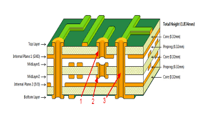
Optimizing Stackup and Material Selection for Faster Turnaround
The choice of materials and stackup configuration plays a major role in PCB fabrication speed. Using readily available materials and standardized stackup designs helps reduce procurement delays and manufacturing complexity. When engineers select common FR-4 materials and proven layer structures, manufacturers like FastTurn PCB can begin production without waiting for special components or extended sourcing cycles. This significantly improves overall project timelines.
Material optimization also affects signal performance and thermal reliability, especially in high-density multilayer boards. A balanced stackup ensures controlled impedance and stable electrical performance, reducing the need for post-production fixes. In quick turn pcb assembly projects, these decisions become even more critical because there is little room for rework. By choosing the right materials early, teams can achieve both speed and quality in a single streamlined process.
Streamlining Via Technology and Drilling Strategies
Vias are essential in multilayer PCB design, but they can also introduce delays if not properly optimized. Traditional through-hole vias are reliable, but advanced designs often benefit from blind or buried vias to save space and improve signal performance. However, complex via structures require more precise drilling processes, which can slow down production if not carefully planned. FastTurn PCB uses optimized drilling strategies to balance performance with manufacturing efficiency.
Reducing unnecessary via complexity is another effective way to accelerate production cycles. By simplifying routing and minimizing via transitions, engineers can significantly reduce fabrication time. This is especially important in quick turn pcb assembly projects, where drilling and lamination steps must be completed quickly without sacrificing accuracy. A well-optimized via strategy ensures faster layer alignment and improves overall production flow across multilayer boards.
Leveraging Quick Turn PCB Assembly Workflows for Rapid Prototyping
Quick turn pcb assembly plays a key role in speeding up the development of multilayer boards, especially during prototyping stages. It allows engineers to test designs in real-world conditions without long waiting periods. FastTurn PCB specializes in these fast-paced workflows, helping companies move from concept to functional prototype in a matter of days. This rapid feedback loop is essential for improving design accuracy and reducing time-to-market.
By integrating assembly and fabrication into a single streamlined process, manufacturers can eliminate delays caused by external coordination. This approach reduces handoff errors and ensures that both PCB fabrication and component assembly are aligned. With quick turn pcb assembly services, engineers can quickly identify issues, make improvements, and move into final production with confidence. This agile workflow is now a standard requirement in competitive electronics markets.
Improving Communication and DFM Checks with Manufacturers like FastTurn PCB
Clear communication between engineers and manufacturers is one of the most effective ways to reduce fabrication delays. When design files are shared with complete specifications and accurate documentation, manufacturers can begin production without uncertainty. FastTurn PCB emphasizes collaborative DFM reviews to ensure that potential issues are identified before fabrication begins, reducing costly revisions later in the process.
Strong collaboration also improves decision-making during critical stages of multilayer PCB production. Engineers can receive real-time feedback on design feasibility, material selection, and layer configuration. This is particularly important in quick turn pcb assembly environments, where small misunderstandings can lead to significant delays. By maintaining open communication channels, teams can ensure smoother workflows and faster project completion.
Reducing Re-spins Through Testing, Validation, and Quality Control
Re-spins are one of the biggest causes of delays in multilayer PCB fabrication, often resulting from design errors or incomplete validation. By implementing thorough testing and simulation before production, engineers can significantly reduce the risk of errors. FastTurn PCB supports detailed quality control processes that help identify potential issues early, ensuring that boards meet performance requirements before full-scale manufacturing begins.
Effective validation also includes electrical testing, signal integrity checks, and prototype evaluation under real conditions. These steps are essential in quick turn pcb assembly projects, where fast feedback is needed to refine designs. By investing time in proper testing upfront, manufacturers and engineers can avoid repeated fabrication cycles, saving both time and cost while improving overall product reliability.
Conclusion
Accelerating multilayer PCB fabrication cycles requires a combination of smart design, efficient manufacturing strategies, and strong collaboration between engineers and manufacturers. By focusing on manufacturability, optimized stackups, simplified via structures, and early validation, teams can significantly reduce production delays while maintaining high-quality standards. Companies like FastTurn PCB play an important role in supporting these fast-paced development needs through advanced processes and reliable expertise.
Ultimately, success in modern electronics depends on how quickly ideas can move from design to functional product. With the help of quick turn pcb assembly services and well-structured workflows, businesses can shorten development cycles and respond faster to market demands. By applying these best practices consistently, teams can achieve both speed and precision, ensuring that multilayer PCB projects are delivered efficiently and reliably every time.